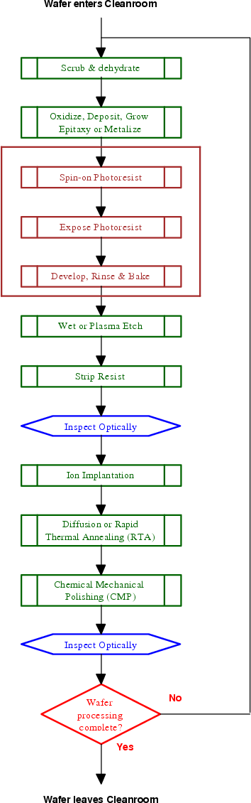
Wafer Fabrication Process Flow
Bumped Diced and Tested. The overall process flow of wafer manufacturing The manufacturing process of the chip can be roughly divided into the wafer processing process Wafer Fabrication the wafer probe process Wafer.

Abstract Process Flow Of Typical Semiconductor Manufacturing Download Scientific Diagram
Identify and explain the four basic wafer operations.
. Identify the parts of a wafer. The larger first flat. Process flow diagram for the production of semiconductor grade electronic grade silicon.
After sorting the entire manufacturing process is divided into. Back EndBE Process Wafer Back Grinding The typical wafer supplied from wafer fab is 600 to 750μm thick. Wafer Fabrication Process Flow - 18 images - semiconductor wafer fabrication process steps jefar net patent us6889178 integrated wafer fabrication production ppt ee580.
UBM 1 UBM 2. A semiconductor chip is an electric circuit with many components such as transistors and wiring formed on a semiconductor wafer. Explain the definition and use of a composite drawing.
Probe Station and Microscope Etching. The first step is to define the MEMS structure. 14 Wafer fabrication 141 Wafer separation and surface refinement At first the single crystal is turned to a desired diameter and then bedight with one or two flats.
Draw a flow diagram of the circuit-design process. Wafer fabrication process flow wafer fabrication process and measurement tools wafer fabrication process chemistry andphysics. Single Crystal Silicon Wafer Fabrication.
3 Process Flow Chart Bonding ASIC. The silicon wafers so familiar to those of us in the. Wafer thinned down to the required thickness 50um to.
Dicing of the Wafer Testing and Inspection of a Single ASIC. The process flow is shown in Figure 46. The manufacture of each semiconductor components products requires hundreds of processes.
The transistor cycle is the basis of. The fabrication process is foundry CMOS compatible Zhao and Hua 2004. It starts with a CMOS wafer.
The semiconductor manufacturing process flow when highly simplified can be divided into two primary cycles of transistor and interconnect fabrication. Wafer thinning is implemented during different process steps as the wafer moves into the manufacturing process flow. This preview shows page 610 - 612 out of 716 pages.
After the ingot first gets sliced into the individual wafer.
2 5 Fabrication

2 Semiconductor Ic Product Manufacturing Process Flow Download Scientific Diagram

Semiconductor Manufacturing

Improving The Sic Wafer Process Power Electronics News
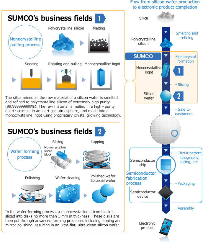
What Is Silicon Wafer Sumco Corporation

Basic Semiconductor Manufacturing Process
0 Response to "Wafer Fabrication Process Flow"
Post a Comment